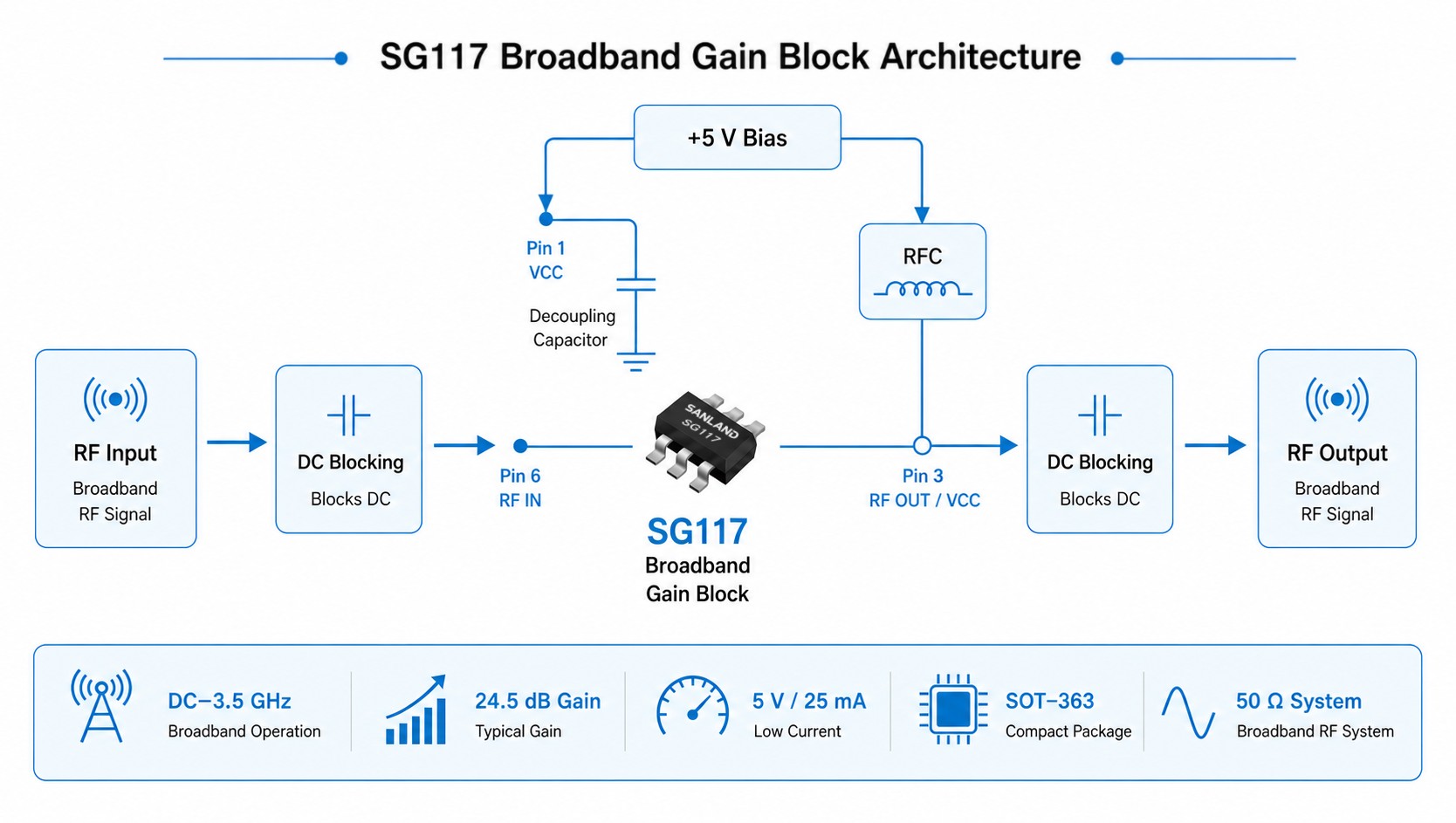
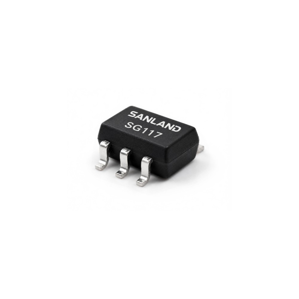
SG117 is a GaAs pHEMT broadband amplifier designed for general-purpose wideband RF amplification from DC to 3.5 GHz. Combining high gain, low noise, high linearity and unconditional stability in a compact 6-pin package, SG117 is suitable for RF front ends, buffer amplifiers and gain stages in wireless, broadband and satellite communication systems. Its single 5 V supply and compact SOT-363 form factor help simplify integration into space-constrained RF designs.
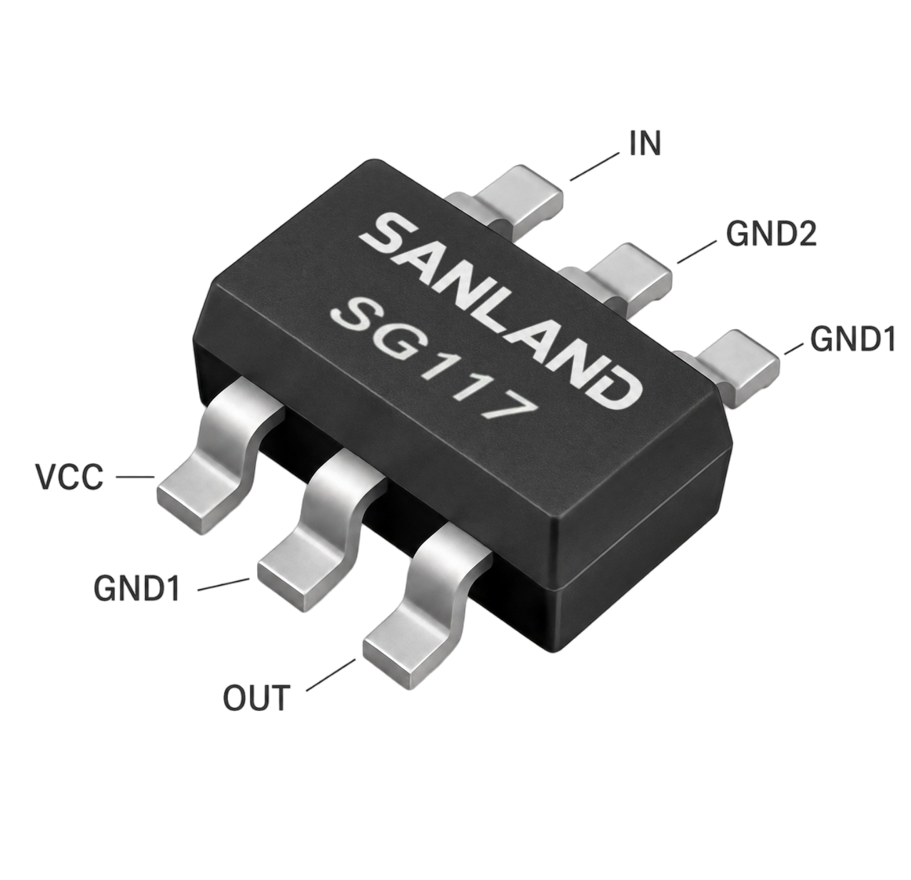
Pin Assignment & Package
Pin
Function
Description
1
VCC
Bias voltage for input gate
2, 4, 5
GND
GND
3
RF OUT / VCC
RF output; apply VCC through RF choke; DC blocking capacitor required
6
RF IN
RF input; DC blocking capacitor required
Body Size: 2.2 × 1.35 × 1.1 mm Max.
The compact 6-pin SOT-363 package makes SG117 suitable for broadband MMIC amplifier designs where PCB space is limited.
Legacy RF design evaluation
Evaluating an Alternative to BGA2866 or BGA2867?
SG117 is a 5 V, SOT-363 broadband RF amplifier covering DC to 3.5 GHz. It can be considered for engineering evaluation in selected legacy BGA2866 and BGA2867 designs. The required gain, noise figure, output performance and existing bias circuit should be reviewed for the intended application.
DC–3.5 GHz5 V supplySOT-363 package
NXP reference part
BGA2866 designs
NXP specifies 23.9 dB typical gain at 950 MHz. SG117 is listed at 24.5 dB at 1 GHz. Use these as starting points and compare the gain response over your actual frequency band.
Current check: 17.4 mA for BGA2866 versus 25 mA typical for SG117, both at 5 V.
NXP reference part
BGA2867 designs
NXP specifies 27.1 dB typical gain at 950 MHz. SG117 is listed at 24.5 dB at 1 GHz. Check whether the available system gain margin meets your requirements.
Current check: 21.7 mA for BGA2867 versus 25 mA typical for SG117, both at 5 V.
Published typical values above use different test frequencies and evaluation conditions. Compare devices at the same frequencies in the intended circuit.
Critical check: output bias circuit
SG117 uses pin 3 for RF OUT / VCC and requires an RF choke for output bias. BGA2866 and BGA2867 list pin 3 as RF_OUT and do not require an output inductor. Review the PCB connections, bias components and DC blocking capacitors before evaluating a substitution.
What to verify in your design
RF performanceGain, NF, P1dB and OIP3 across the operating band.
Circuit and supplyOutput bias, DC blocking, current budget and thermal margin.
Sourcing needsQualification timeline and estimated annual demand.
Request a cross-reference review
Send your original part number, frequency range, target gain/NF, linearity requirements, schematic or BOM (if available), and annual quantity to the SANLAND engineering team.
SG117 is designed for broadband RF amplification from DC to 3.5 GHz.
What supply voltage does SG117 require?
SG117 is a 5 V RF gain block amplifier with a typical quiescent current of 25 mA, making it suitable for compact and low-current RF designs.
What package does SG117 use?
SG117 is supplied in a compact 6-pin SOT-363 package suitable for space-constrained RF designs.
What applications is SG117 designed for?
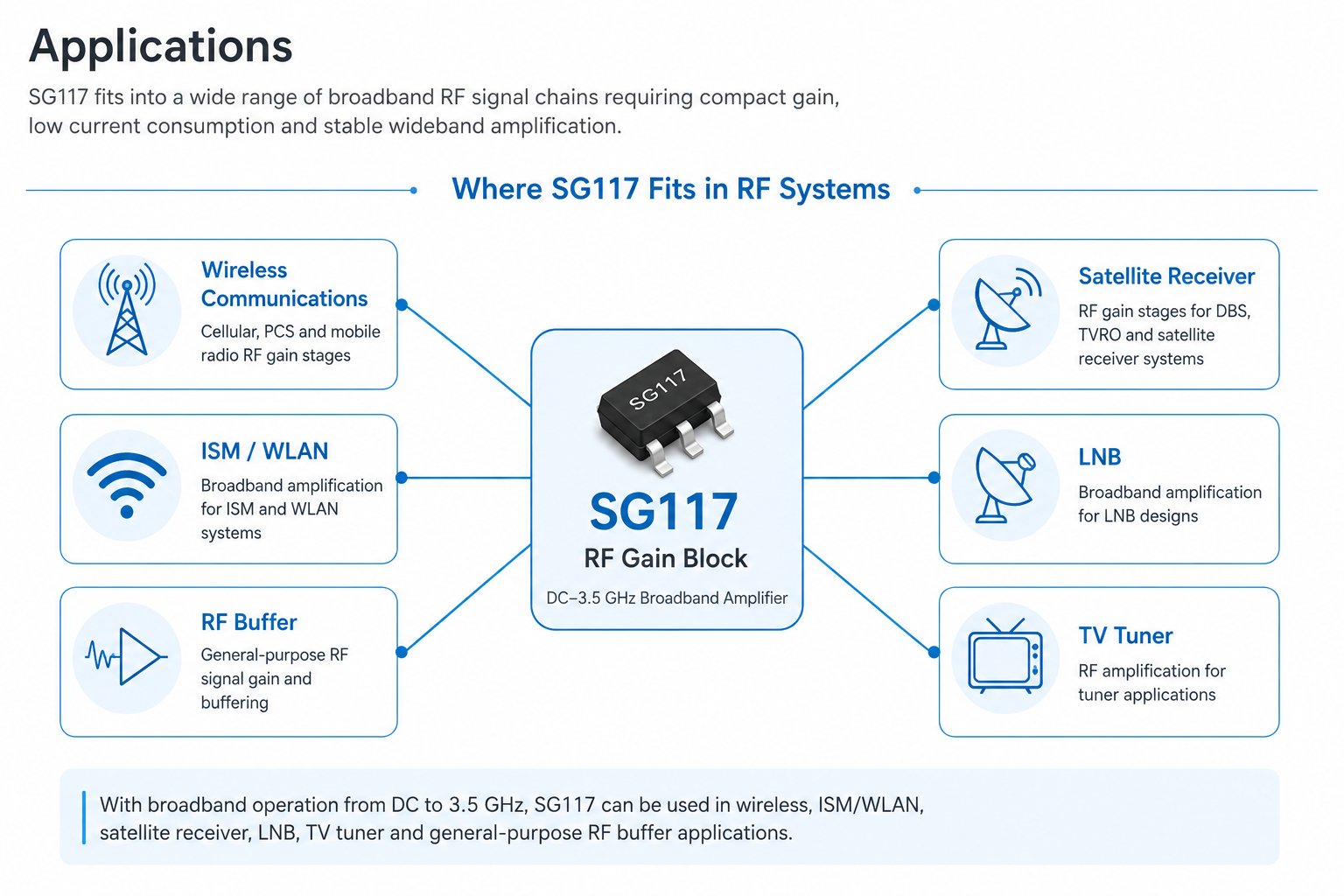
SG117 can be used in broadband RF gain stages for wireless communications, ISM and WLAN systems, DBS/TVRO, RF front ends, buffer amplifiers and tuner applications.
Can SG117 be evaluated for legacy broadband MMIC designs?
Yes. SG117 may be considered for engineering evaluation when migrating from selected legacy SOT-363 broadband MMIC gain blocks, including NXP BGA2866, BGA2867 and BGA2869. Circuit configuration, bias network, gain requirements and RF performance should be independently verified for each application.
01
SG117 / RF SPECIFICATIONS
RF Performance
Parameter
Typical Value
Test Condition
Frequency Range
DC–3.5 GHz
—
Gain
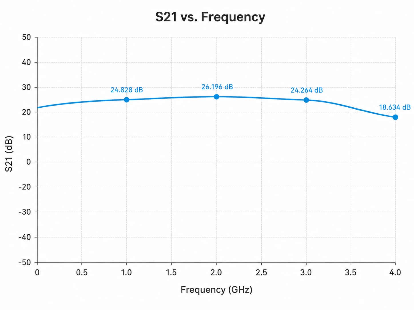
24.5 dB
@ 1 GHz
Noise Figure
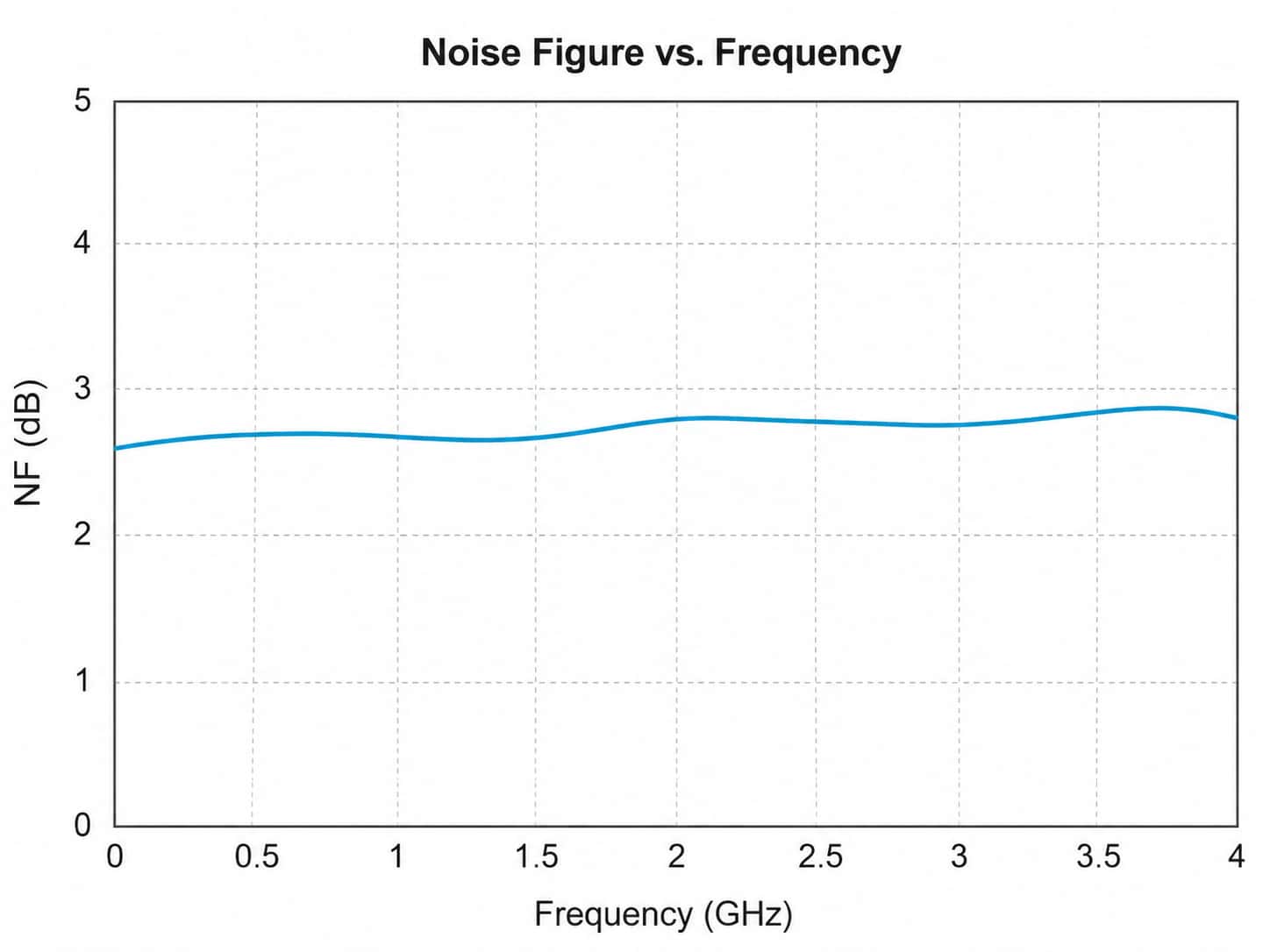
2.7 dB
@ 1 GHz
OIP3
+21 dBm
@ 1 GHz
Output P1dB
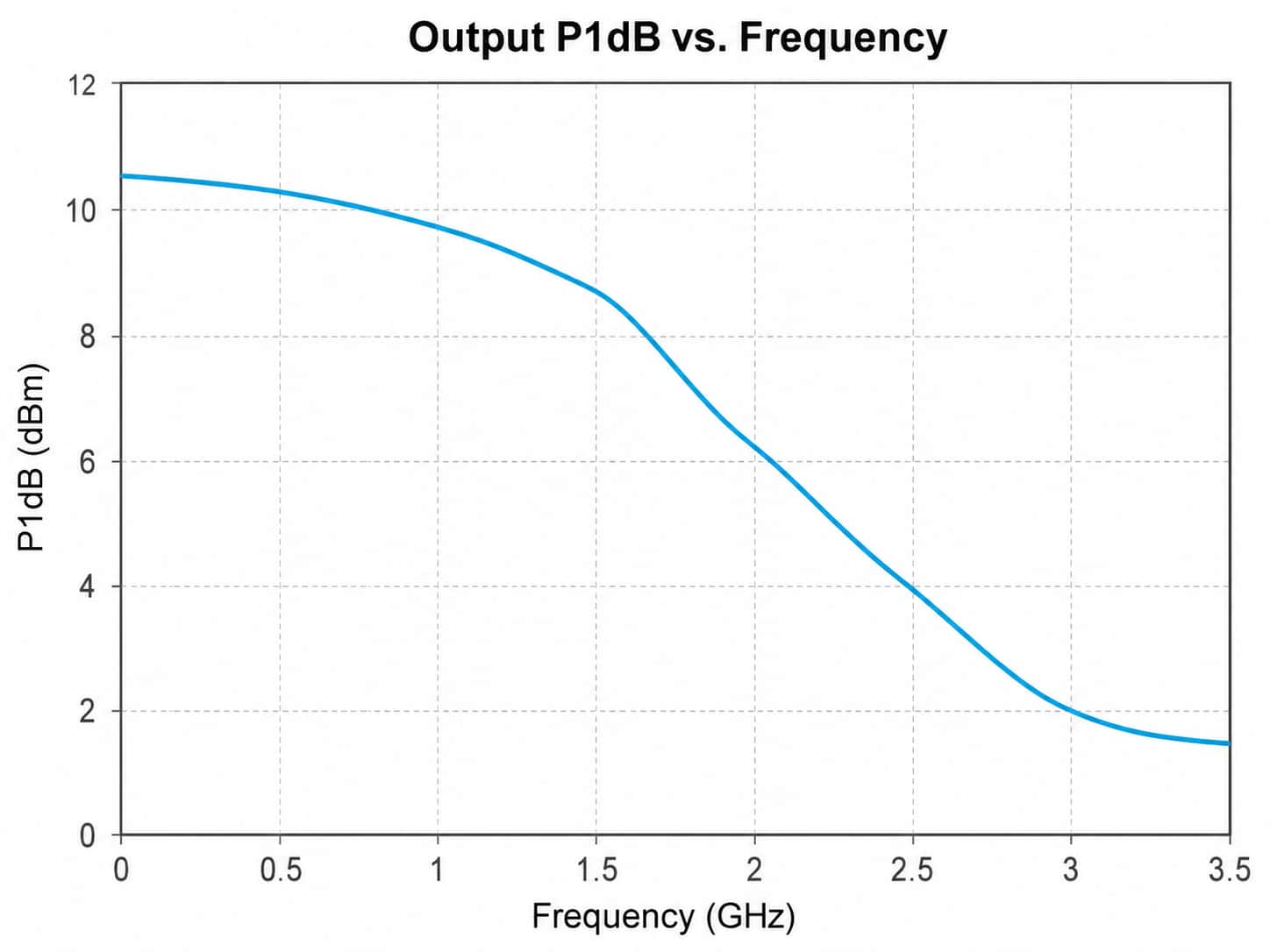
+10 dBm
@ 1 GHz
S11
–14 dB
@ 2.5 GHz
S22
–12 dB
@ 2.5 GHz
S12
–32 dB
@ 2.5 GHz
Supply Voltage
5 V
—
Supply Current
25 mA Typ.
—
System Impedance
50 Ω
Test condition
Package
SOT-363
6-pin
TEST BASIS
Typical RF performance is characterized in a 50 Ω system with a 5 V supply, providing reference data for broadband gain block selection and RF design.
02
SG117 / MEASURED CURVES
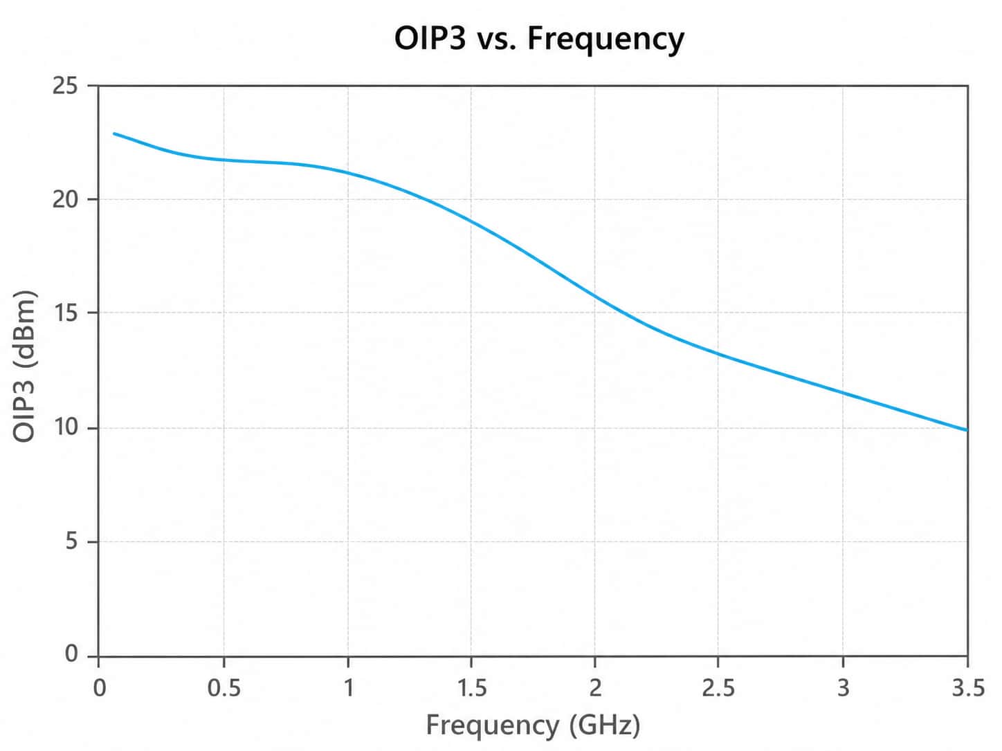
Typical RF Performance vs. Frequency
01S21Forward transmission
02Noise FigureNoise response
03Output P1dBOutput compression
04OIP3Linearity response
SG117 can be used as a broadband RF buffer amplifier and MMIC gain block for RF front-end applications, including wireless communications, ISM/WLAN systems, satellite receivers, LNBs and TV tuners. Its DC–3.5 GHz broadband response supports general-purpose RF gain and buffering across a wide range of signal chains.


 English
 français
 Deutsch
 русский
 español
 português
 日本語
日本語 한국의
한국의 العربية
 中文
中文




 IPv6 network supported 粤ICP备19046464号